eMCP desoldering is a high-end hardware hacking method used when software access is blocked, since eMCP packages combine both NAND storage and DRAM in a single BGA chip. By removing the package, researchers can dump raw data, bypass secure boot, or attempt forensic recovery. Other chip types also come into play: eMMC and UFS (storage-only) are common BGA targets for firmware extraction, while uMCP integrates UFS with RAM and raises the complexity further. LPDDR RAM itself isn’t directly useful for dumping but can be attacked through side channels like cold boot. PoP packages, where the CPU and memory are stacked, add another layer of difficulty for direct analysis. On the easier side, raw NAND or NOR flash chips sometimes appear in TSOP, SOIC, or WSON packages, and SPI NOR boot flash in SOIC-8 is especially hacker-friendly since it can be clipped or desoldered for straightforward reads. In practice, this means modern smartphones and IoT devices force hackers to deal with challenging BGA chip-off work, while older or low-end hardware often exposes more accessible packages that are quicker to attack.
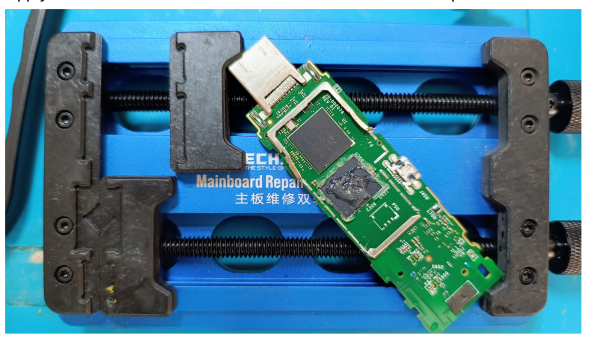
Note: This blog is completely for educational purposes only. We have chosen the target device Amazon Firestick 1st Generation which has the eMCP.
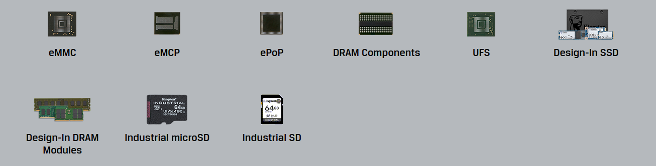
| Chip Type | Definition / What It Is | Hacker’s POV |
|---|---|---|
| eMMC (embedded MultiMediaCard) | Storage chip (NAND + controller) in BGA. Used in phones, IoT, embedded systems. | Common chip-off target for firmware dumps. |
| eMCP (embedded Multi-Chip Package) | Combines NAND storage + DRAM in one BGA package. Space-saving design for mobile/IoT. | Harder to rework; used for deep data extraction and bypassing secure boot. |
| UFS (Universal Flash Storage) | Faster, newer storage standard than eMMC. Always BGA. | Requires advanced adapters/programmers; tougher than eMMC. |
| uMCP (UFS Multi-Chip Package) | Combines UFS storage + RAM in one BGA. | Even more complex; tricky for hackers to separate functions. |
| LPDDR / DRAM Components | Low-power DDR RAM chips, memory only. | Not for dumping, but exploitable with cold boot or fault attacks. |
| PoP / ePoP (Package on Package) | CPU and RAM stacked in a single BGA package. | Extremely hard to access; usually avoided unless advanced probing. |
| Raw NAND Flash | Bare NAND storage without controller. Can be BGA or TSOP. | Useful for direct dumps but needs ECC handling. |
| NOR Flash | Smaller, faster storage, often used for boot firmware. Comes in SOIC, TSOP, or BGA. | Good for bootloader extraction or reverse engineering. |
| SPI NOR Flash | Serial NOR flash, often in SOIC-8 or WSON packages. Stores BIOS/boot code. | Hacker-friendly: easy to clip or desolder and dump. |
| Design-In SSD | Embedded solid-state drives (NAND + controller in SSD form factor). | Easy to interface with standard tools, but firmware hacking can be complex. |
| Design-In DRAM Modules | Full DRAM modules (like SO-DIMM, industrial/embedded boards). | Not for direct dumping, but can be attacked with side-channel/fault methods. |
| Industrial microSD | Removable flash storage card in microSD form factor. | Very easy to dump with off-the-shelf card readers. |
| Industrial SD | Same as microSD but full-size SD card form factor. | Also easy to dump; common in industrial/embedded gear. |
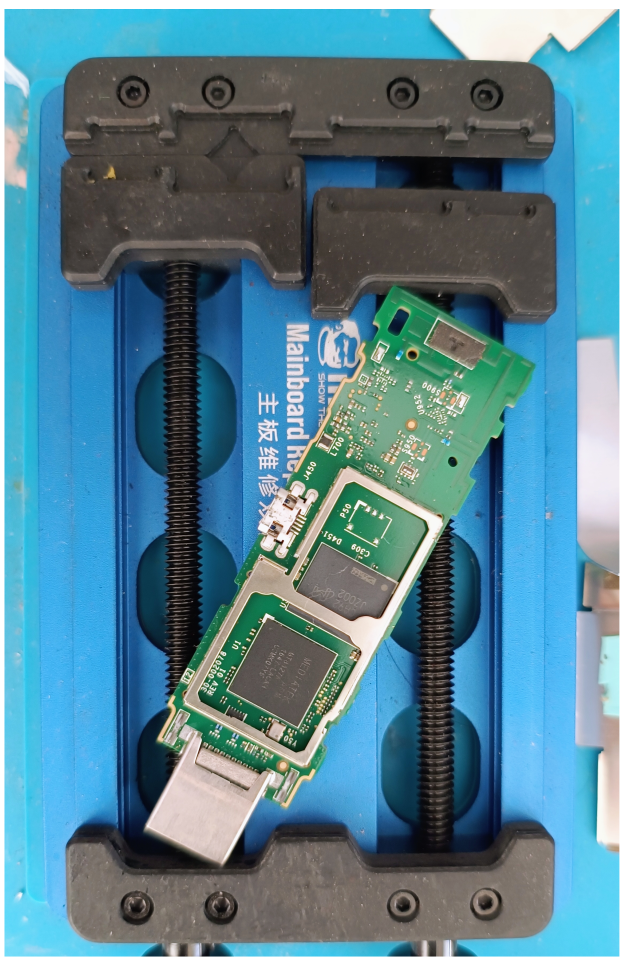
Step 1: Secure the PCB in a Holder
Before proceeding with eMMC chip removal, stabilize the board to prevent accidental damage.
- Method: Use a sturdy mechanical holder.
- Affordable, reliable support, minimizes movement during desoldering/reballing.
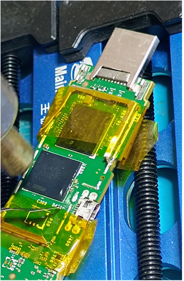
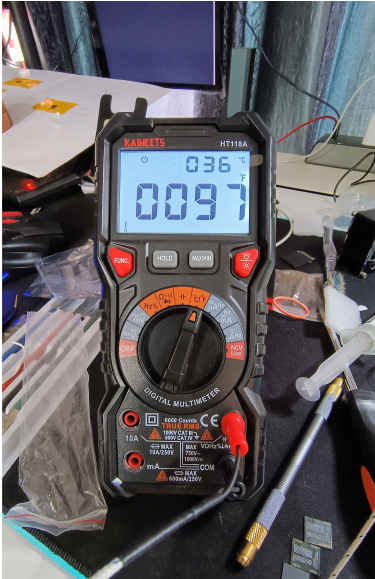
Step 2: Identifying Faulty BGA (Ball Grid Array) Chips
Inspect for faulty eMMC chips before removal:
- Visual Inspection: Check for cracks, discoloration, or misalignment.
- Thermal Imaging: Detect hotspots indicating poor connections.
- Multimeter/Continuity Test: Identify open/short circuits.
- X-ray (if available): Examine solder ball integrity non-destructively.
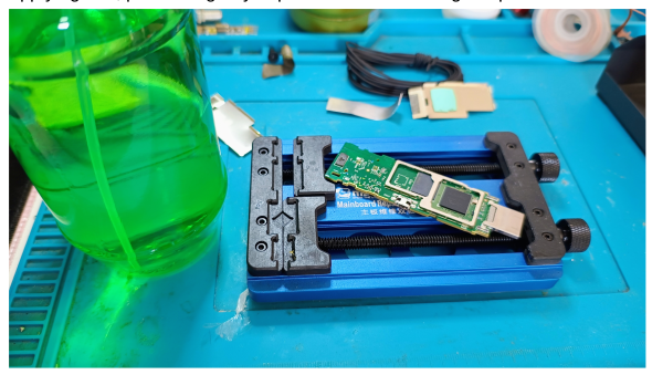
Step 3: Cleaning the Area Around the eMMC
Goal: Remove dust/flux residues for better heat distribution.
- Surface Cleaning: Wipe with isopropyl alcohol (IPA) and lint-free cloth.
- Chip Cleaning: Post-removal, clean residual solder with solder wick.
- PCB Cleaning: Use desoldering braid + IPA on pads for fresh solder adhesion.
Step 4: Applying Minimal Flux
Purpose: Prevents oxidation, ensures proper solder wetting.
- Tools: Flux pen/syringe.
- Technique:
- Apply thin, even layer on eMMC.
- Avoid overapplication (prevents solder bridges).
- Keep flux confined to target area.
Step 5: Applying Kapton Tape
Why? Protects nearby components from heat damage.
- Steps:
- Cut tape to size, wrap around eMMC.
- Smooth for adhesion (no gaps).
- Verify tape doesn’t obstruct soldering area.
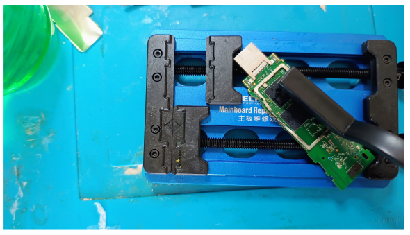
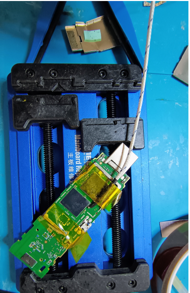
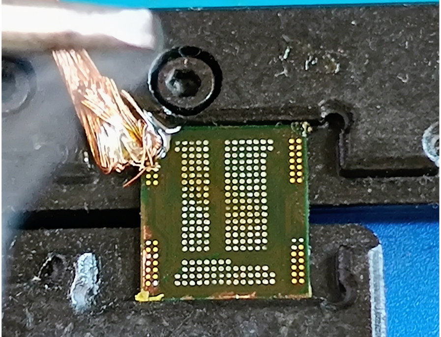
Step 6: Removing the BGA (eMMC) Chip
Tools: Hot air rework station, thermocouple, tweezers.
- Heating:
- Monitor temperature (solder melts at 138°C or 183°C - check with datasheets relative chip model).
- Bubbles at 110–120°C indicate low-temp solder.
- Lifting:
- Use tweezers/vacuum tool when solder is molten.
- Avoid force to prevent pad damage.
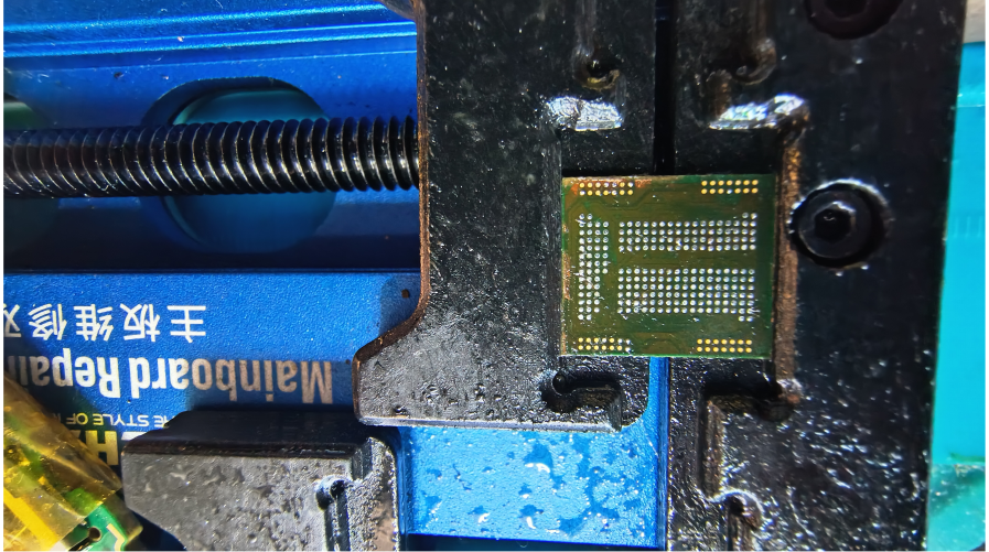
Step 7: Desoldering Process
Goal: Clean PCB pads for reballing.
- Soldering Iron: Set to 300–350°C.
- Desoldering Wick:
- Place on pads, heat with iron.
- Move wick in a "7:30" clockhand motion.
- Inspect Pads: Clean with IPA; ensure flat, residue-free surface.
Step 8: Cleaning with Haired Brush & IPA
Steps:
- Dip soft brush in 99% IPA.
- Gently scrub pads/chip in circles.
- Wipe dry with lint-free cloth.
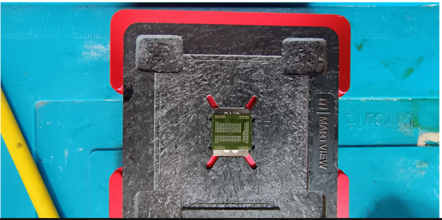
Step 9: Reballing the eMMC Chip
9a. Applying Flux
- Thin layer on chip pads. Avoid excess.
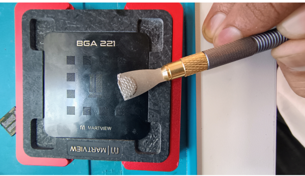
9b. Stencil Placement
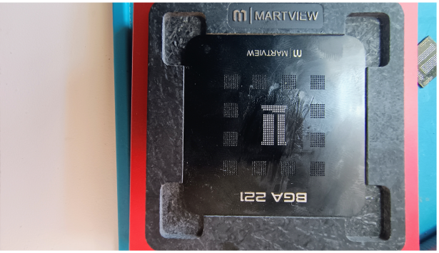
- Align BGA stencil (use magnetic holder for precision).
- Tool Tip: RB-01 reballing station recommended.
9c. Solder Ball Placement
Method 1: Pre-made Solder Balls
- Fill stencil openings with balls.

Method 2: Solder Paste
- Press paste on lint-free cloth to dry.
- Apply paste in "4:00" motion, remove excess at "10:00".
Final Checks:
- Reheat to shape balls if needed.
- Ensure no bridges (critical for adapter compatibility).
Conclusion
This concludes Part 1 of our eMMC/eMCP removal and reballing guide.
In Part 2, we’ll explore data extraction, adapter alignment, and dump analysis - critical steps for successful chip-off recovery and secure boot bypass attempts.
Always remember: this process is destructive and should be performed on test hardware only.